(China (Mainland))

Product Summary
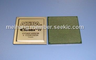
The EP2S60F1020C5N is an FPGA. It is based on a 1.2-V, 90-nm, all-layer copper SRAM process and features a new logic structure that maximizes performance, and enables device densities approaching 180,000 equivalent logic elements (LEs). The EP2S60F1020C5N offers up to 9 Mbits of on-chip, TriMatrix memory for demanding, memory intensive applications and has up to 96 DSP blocks with up to 384 (18-bit × 18-bit) multipliers for efficient implementation of high performance filters and other DSP functions. The EP2S60F1020C5N supports various I/O standards along with support for 1-gigabit per second (Gbps) source synchronous signaling with DPA circuitry.
Parametrics
EP2S60F1020C5N absolute maximum ratings: (1)Supply voltage:–0.5V to 1.8V; (2)Supply voltage:–0.5V to 4.6V; (3)Supply voltage:–0.5V to 4.6V; (4)Analog power supply for PLLs:–0.5V to 1.8V; (5)Digital power supply for PLLs:–0.5V to 1.8V; (6)DC input voltage:–0.5V to 4.6V; (7)DC output current, per pin:–25mA to 40mA; (8)Storage temperature:–65℃ to 150℃; (9)Junction temperature:–55℃ to 125℃.
Features
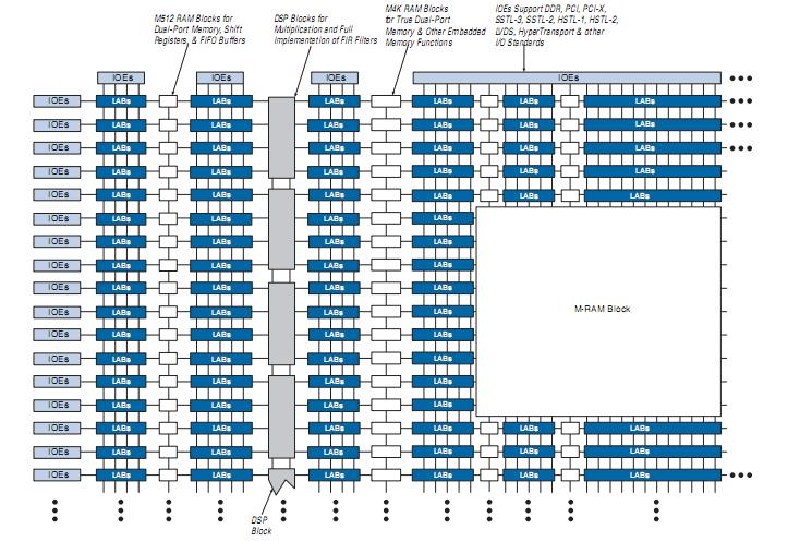
EP2S60F1020C5N features: (1)Support for numerous single-ended and differential I/O standards; (2)High-speed differential I/O support with DPA circuitry for 1-Gbps performance; (3)Support for high-speed networking and communications bus standards including Parallel RapidIO, SPI-4 Phase 2 (POS-PHY Level 4), HyperTransport technology, and SFI-4; (4)Support for high-speed external memory, including DDR and DDR2 SDRAM, RLDRAM II, QDR II SRAM, and SDR SDRAM; (5)Support for multiple intellectual property megafunctions from Altera MegaCore functions and Altera Megafunction Partners Program (AMPPSM) megafunctions; (6)Support for design security using configuration bitstream encryption; (7)Support for remote configuration updates; (8)15,600 to 179,400 equivalent LEs; (9)New and innovative adaptive logic module (ALM), the basic building block of the Stratix II architecture, maximizes performance and resource usage efficiency; (10)Up to 9,383,040 RAM bits (1,172,880 bytes) available without reducing logic resources; (11)TriMatrix memory consisting of three RAM block sizes to implement true dual-port memory and first-in first-out (FIFO)buffers; (12)High-speed DSP blocks provide dedicated implementation of multipliers (at up to 450 MHz), multiply-accumulate functions, and finite impulse response (FIR) filters; (13)Up to 16 global clocks with 24 clocking resources per device region.
Diagrams
| Image | Part No | Mfg | Description |  |
Pricing (USD) |
Quantity | ||||||
|---|---|---|---|---|---|---|---|---|---|---|---|---|
 |
 EP2S60F1020C5N |
|
IC STRATIX II FPGA 60K 1020-FBGA |
Data Sheet |
|
|
||||||
| Image | Part No | Mfg | Description | |
Pricing (USD) |
Quantity | ||||||
 |
EP2S |
Other |
|
Data Sheet |
Negotiable |
|
||||||
|
EP2S130F1020C3 |
|
IC STRATIX II FPGA 130K 1020FBGA |
Data Sheet |
|
|
||||||
|
EP2S130F1020C3N |
|
IC STRATIX II FPGA 130K 1020FBGA |
Data Sheet |
|
|
||||||
|
EP2S130F1020C4 |
|
IC STRATIX II FPGA 130K 1020FBGA |
Data Sheet |
|
|
||||||
|
EP2S130F1020C4N |
|
IC STRATIX II FPGA 130K 1020FBGA |
Data Sheet |
|
|
||||||
|
EP2S130F1020C5 |
|
IC STRATIX II FPGA 130K 1020-FBG |
Data Sheet |
|
|
||||||